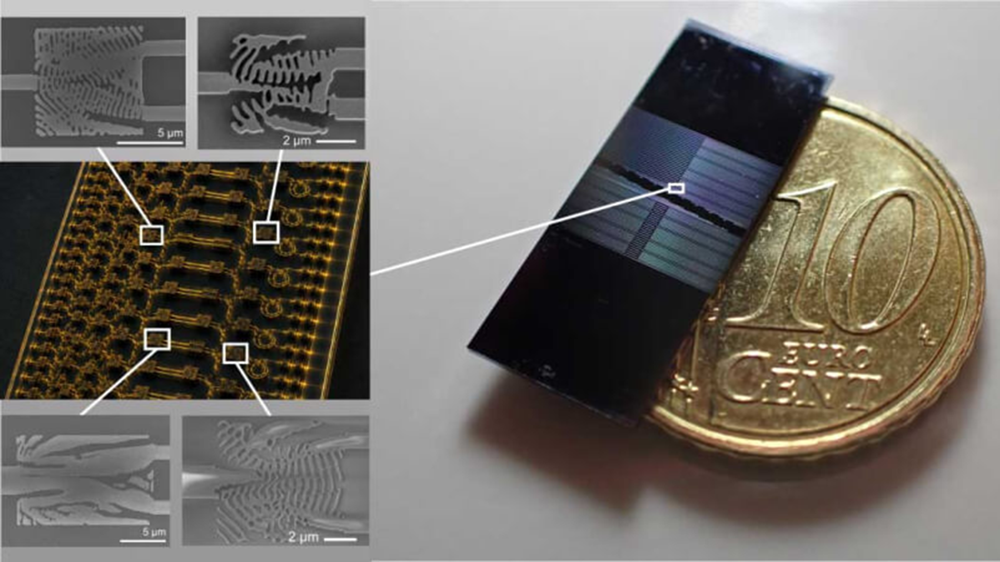
Researchers at the Max Planck Institute for the Science of Light used an artificial intelligence algorithm to design three photonic chip components that are up to 500 times smaller than conventional hand-engineered versions. The components — a wavelength splitter, a spatial mode sorter, and a mirror — measure just a few micrometers across, roughly the size of a single bacterium. The work was published May 28 in Nature Communications.
Photonic microchips use photons instead of electrons to transmit and process data, offering higher speed, greater bandwidth, and lower heat loss. They rely on micrometer-wide waveguides to direct light, along with components that separate wavelengths, sort spatial modes, and reflect light. Shrinking these elements frees space for additional on-chip functionality.
The team employed an inverse-design approach: they specified the desired optical behavior and manufacturing constraints, then let the algorithm iteratively optimize nanostructure geometries. The resulting designs are described as beyond human intuition, with complex shapes no engineer would likely draw. The same framework produced all three component types on the same material platform.
Fabrication used relatively thick silicon nitride, 400 to 800 nanometers, which confines light more strongly and reduces loss compared with standard silicon. The mirrors, about 11 micrometers long, reflected up to 98.5% of incoming light while suppressing unwanted modes. Light bounced between paired mirrors over 100 times before escaping, indicating low propagation loss.
The wavelength splitter measures approximately 5 micrometers across, and the spatial mode sorter is marginally larger. Each component was demonstrated individually. The researchers have not yet combined them into a complete integrated optical circuit, which they identify as the next step toward fully functional high-density photonic chips.
The study also highlights that the designs are robust against fabrication errors, a practical requirement for scalable manufacturing. In recent years, AI-driven semiconductor design has shortened development cycles and lowered costs, with some systems generating layouts from brief text prompts. This work extends that trend to nanophotonic component design.
'Beyond human intuition': AI designs chip components 500 times smaller than what engineers could ever imagine
This is an independent summary. The complete reporting, supporting context and any primary documents remain with Live Science.