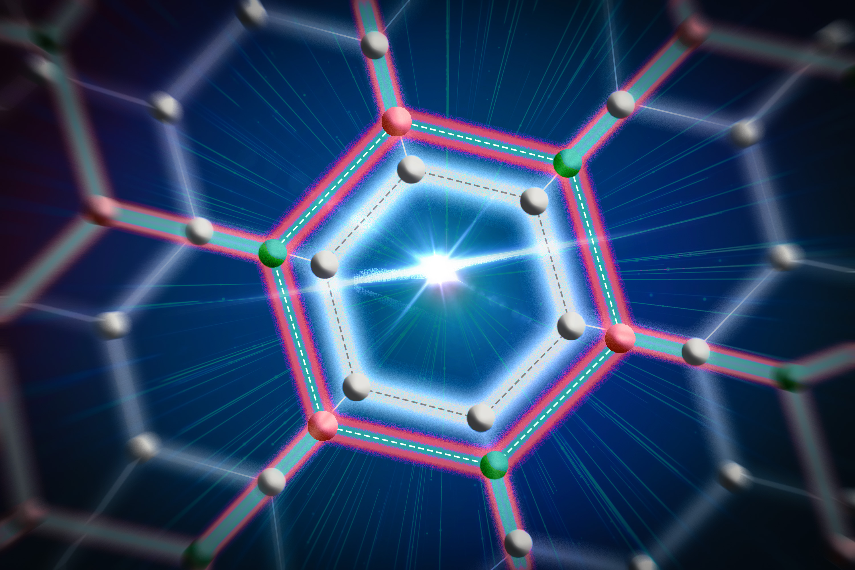
Researchers at MIT and collaborating institutions have developed a method to grow wafer-scale films of niobium diselenide, an ultrathin superconductor only one or a few atoms thick, that remains stable in ambient air. The technique places a layer of graphene on a silicon dioxide substrate before introducing precursor materials, which then form the superconductor in the sub-nanometer gap between the two layers. The graphene encapsulates the material during growth, preventing the rapid oxidation that has previously limited these materials to small, exfoliated flakes.
The resulting niobium diselenide films are smooth, uniform, and continuous over areas larger than one inch. Because the superconductor is already protected by graphene, the researchers can remove the structure into the ambient environment without degradation. They also devised an oxidation-free transfer process to peel the graphene-niobium diselenide stack from its growth substrate and integrate it into a superconducting microwave circuit.
Testing showed the material maintained its superconducting properties and exhibited high kinetic inductance after clean-room fabrication and circuit integration. High kinetic inductance allows a tiny piece of thin-film material to store significant inductive energy, potentially replacing large arrays of Josephson junctions and enabling more compact quantum devices. The researchers demonstrated the growth strategy can extend to a broader family of monolayer quantum materials with diverse properties.
The work, published in Nature, was led by graduate students Xudong Sheldon Zheng and Sameia Zaman, postdoc Kenan Zhang, and professors William D. Oliver, Joel I.-J. Wang, and Jing Kong, with contributions from MIT, Lincoln Laboratory, Rice University, Yale University, and Pohang University of Science and Technology. Funding came from multiple U.S. agencies, the Schlumberger Foundation, the Semiconductor Research Corporation, and the National Research Foundation of Korea.
Previous approaches deposited precursors onto a substrate and then attempted to add a protective layer afterward, but the superconductor began oxidizing almost immediately. By growing the material underneath pre-placed graphene, the team eliminated this degradation window and simplified fabrication. The weak adhesion between graphene and silicon dioxide naturally creates the sub-nanometer gap where the crystal forms.
Making reliable electrical connections to the roughly one-nanometer-thick film posed another challenge. The researchers carefully etched the side walls of the thin-film superconductor in a vacuum chamber to preserve smooth edges, achieving reliable contact with electrodes hundreds of nanometers thick. The integrated circuit maintained the material's high kinetic inductance, a key resource for quantum computing hardware and ultrasensitive detectors.
The advance addresses a long-standing roadblock to studying and utilizing two-dimensional superconductors at practical scales. Researchers can now probe the fundamental physics of these materials and prototype quantum devices using wafer-scale, air-stable films. The team aims to integrate these materials into functional device architectures for quantum computing, communications, and cosmology applications.
Researchers make air-stable, ultrathin superconductors, for more scalable quantum devices
This is an independent summary. The complete reporting, supporting context and any primary documents remain with MIT News.