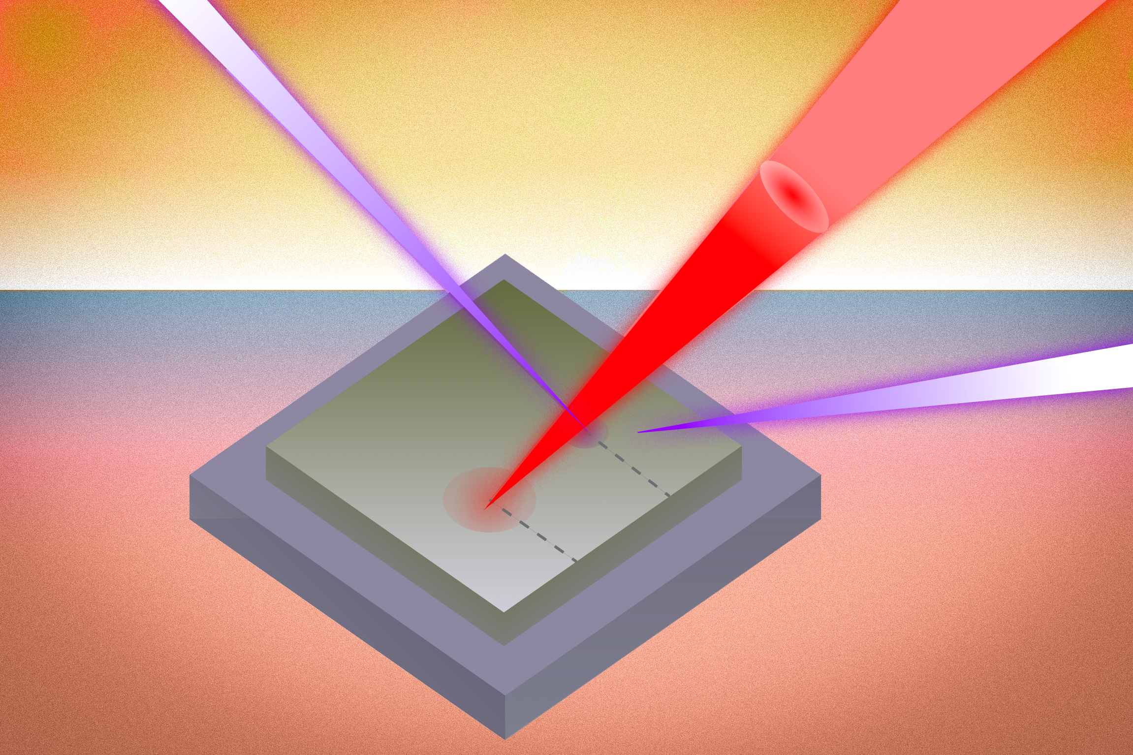
MIT researchers have demonstrated a method for measuring how heat moves through multilayered materials such as computer chips, combining ultrafast X-ray diffraction with laser pulses to track thermal transport at the nanoscale. The work, published in Nature Communications, addresses a longstanding limitation of optical techniques that cannot penetrate buried layers or resolve layer-by-layer heat flow.
The technique uses laser pulses to heat a sample while ultrafast X-rays probe changes in crystal lattice spacing across multiple material layers, capturing how strain evolves as heat dissipates. This provides spatiotemporal maps of thermal transport with fine spatial resolution and the ability to distinguish individual layers in realistic device stacks.
The team applied the method to a test structure of gallium nitride on silicon, a combination studied for high-power and flexible electronics. They measured a fourfold reduction in heat dissipation across a single wrinkle defect in the gallium nitride layer, as well as a 25 percent drop in cross-plane thermal transport, revealing that such common processing defects block heat far more than previously quantified.
The defect also caused anisotropic heat spread, with thermal transport easier in one in-plane direction than another. Researchers say this level of detail was inaccessible with prior methods, which typically yield only averaged signals and cannot resolve buried interfaces or localized defects.
Mingda Li, associate professor of nuclear science and engineering and co-corresponding author, said overheating has become the primary bottleneck for device performance and that the new approach enables direct experimental measurement of thermal flow at the scales where hotspots form. Co-corresponding author Jeehwan Kim, associate professor of mechanical engineering, noted that a leading semiconductor industry consortium has already expressed interest in applying the technique to study commercial chip architectures.
The research was supported by the U.S. Department of Energy, the National Science Foundation, and the MIT School of Engineering Distinguished Energy Efficiency Fellowship. Collaborators included researchers from Argonne National Laboratory and the University of Texas at Austin.
A new way to watch heat move through electronics
This is an independent summary. The complete reporting, supporting context and any primary documents remain with MIT News.